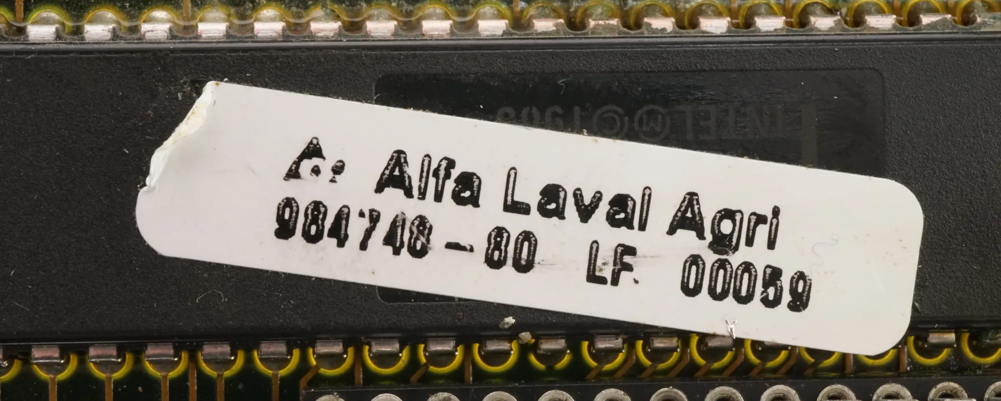
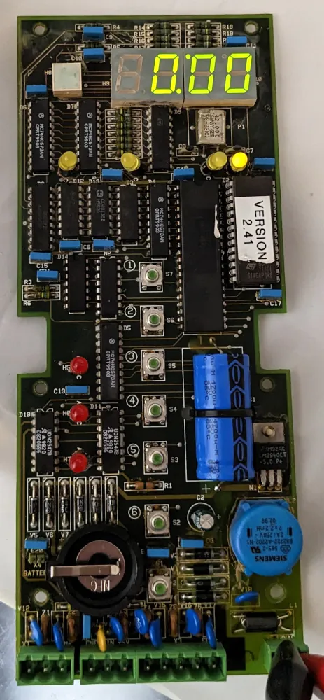
2023-02-22: So I was given this circuit board... And so begins another geeky story... geeky stories aren't quite like other tales - this one is true...and geeks aren't normally good at story-telling (they add too many details) and it might not have a happy ending. All geeks like their circuit boards to be working in the end...but there are some that you just can't get going again. (did I set the expectation low enough yet?). So this particular Printed Circuit Board is labeled as an Alfa Laval Agri 984748-80 LF 00059
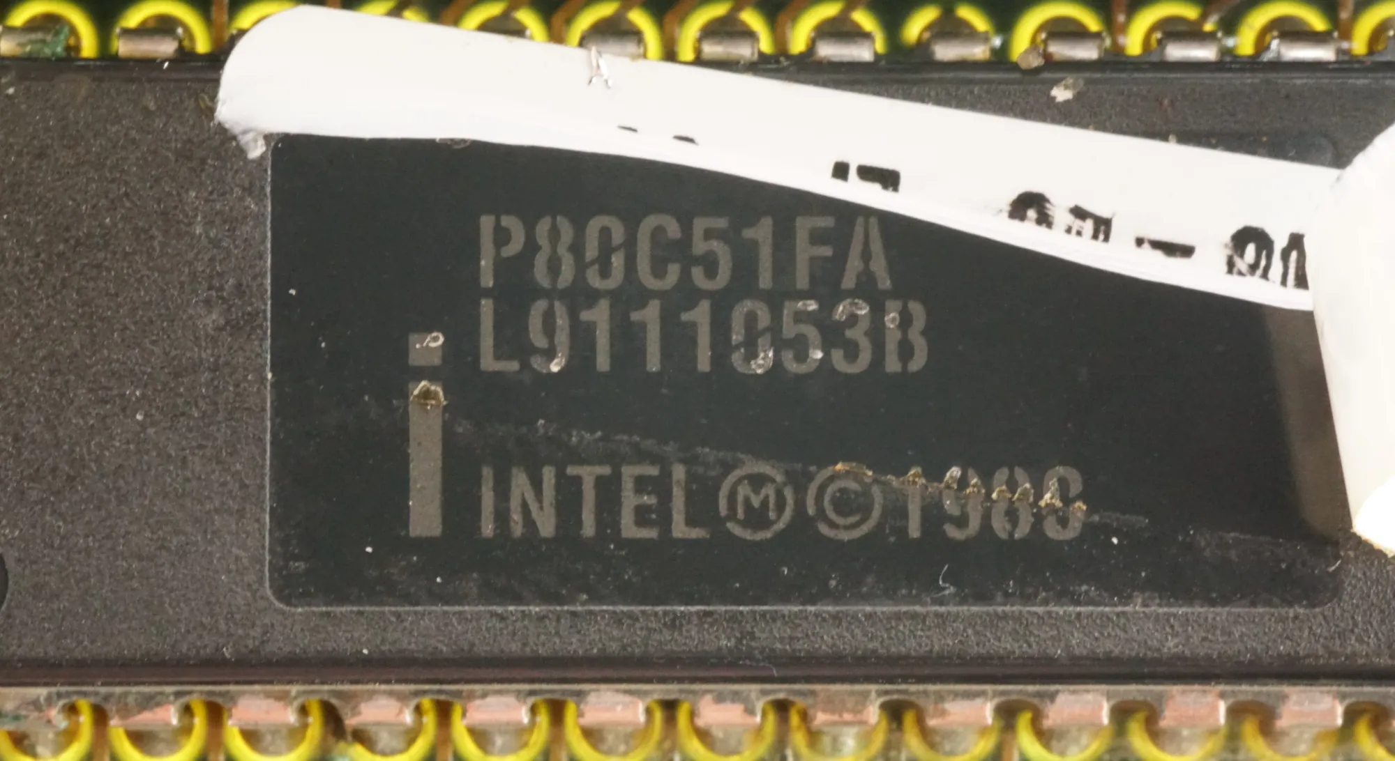
Alfa Laval makes milking equipment, so this board has its home out in a milking barn in an enclosed plastic box (thankfully). This PCB is obsolete, although there is a supposed replacement available (although I can't seem to get any info on it). I can get a rough date on the manufacture time of the board by looking at chips - it was made sometime after the 3rd week of 1999. So of course the first question is: what CPU is being used? And for that, we need to peel a sticker...
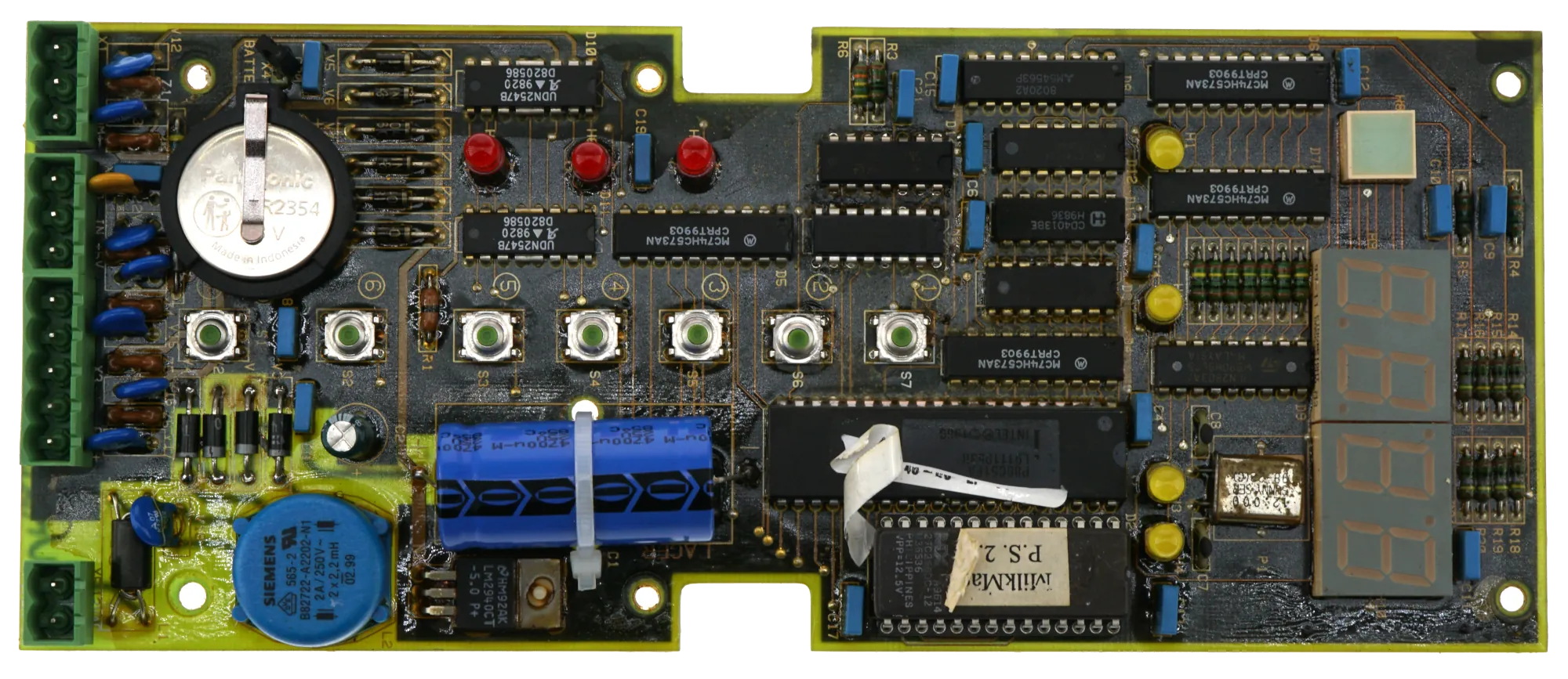
Ahh, a P80C51FA made by Intel. And now, an overview of the board itself would probably be helpful.
After a quick look at the board, you've probably noticed that it appears as if the board has had some components removed and replaced. I was told that another company attempted a repair on the board and returned it marked 'unable to repair'. It looks like D14, N2, all the switches, C1, and V1-V4 (diodes) and the battery have been removed and replaced. Soldering is a little poor quality, but not terrible. On powerup, the board turns on - various LEDs light up and then stop within 250msec or so. What lights up and stays on seems to vary... I don't have all the accessories to check proper function, but I can return the board and have them test it.
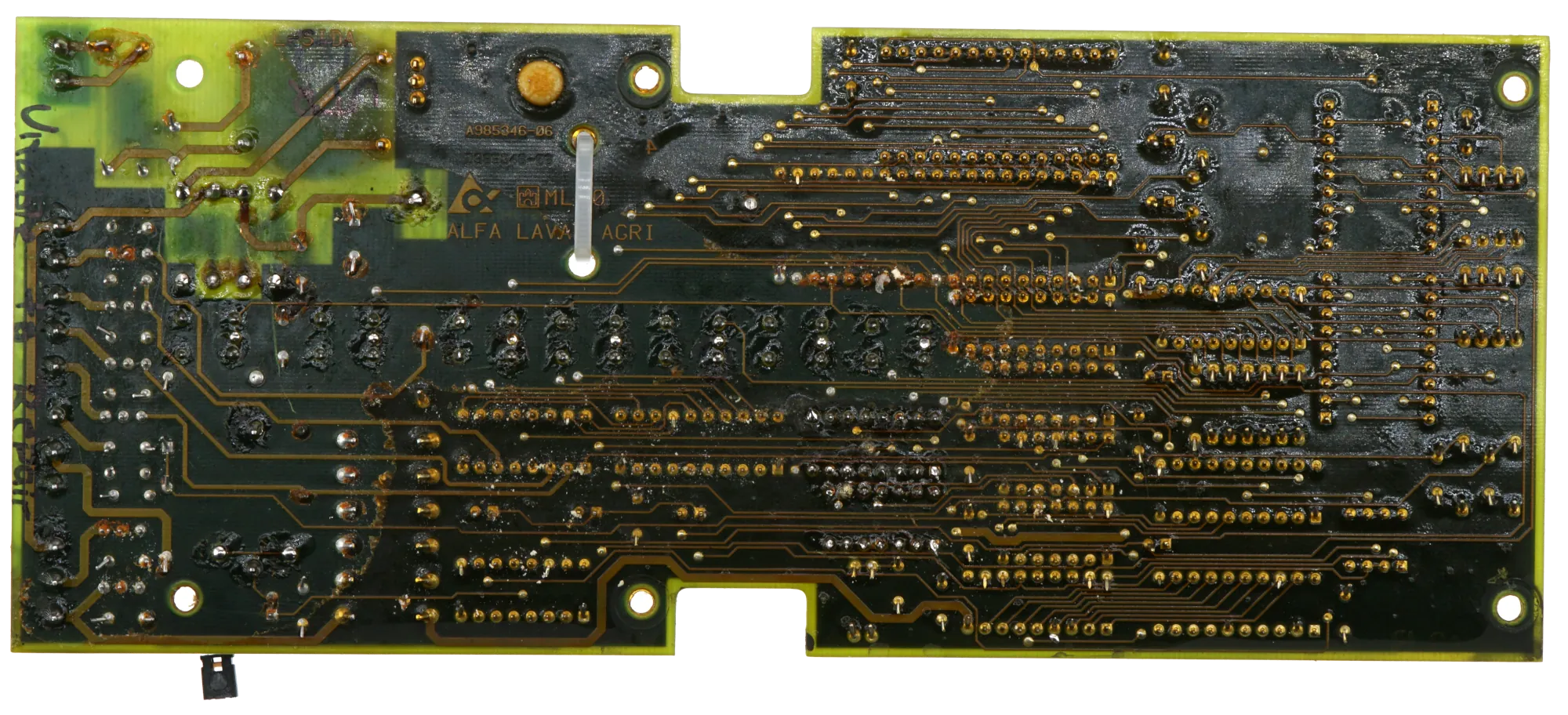
A couple quick notes on the previous repair[s]: Some of the board coating was removed on the bottom of the board around the switches and battery areas; but nothing was touched on the top of the board. Strangely , D14/N2 haven't had the coating removed around them. N2 is the Microprocessor Supervisory Circuit (MAX691ACPE). Seems like this might be a place to start... Diode V2 is missing its connection to V4 (bad solder job). Power in supposedly is a center tapped 12v transformer - I was told to connect +6V to one pin and -6V to the other pin. Center tap gets grounded. This doesn't quite make sense to me though... Power enters and gets sent immediately to the V1 to V4 diode rectifier. Positive output of rectifier diodes gets connected to the COM+ pins. Anyway, I'm going to remove the coating from the board and pull D14/N2...
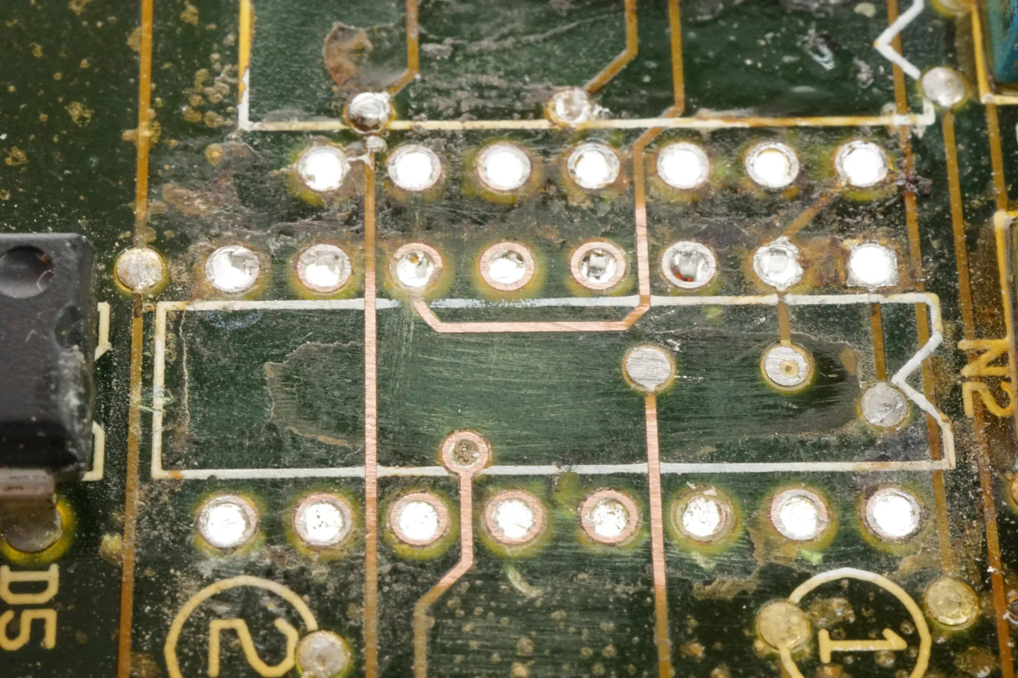
...several days pass... I still don't have the coating fully off the bottom of the board or the top... Lets just pull D14/N2...
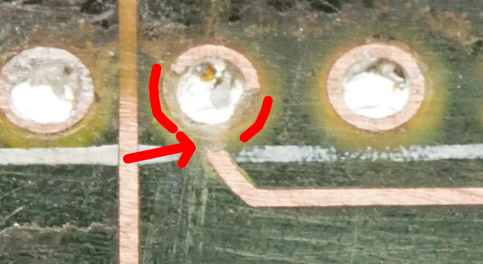
Can you spot it?
Now you can... That is pin 6, which is the LOW LINE System Status Indicator Output. ehh a bodge wire on the bottom of the board can fix that one... that's problem number 2...lets reassemble and test again. ...still same problem...
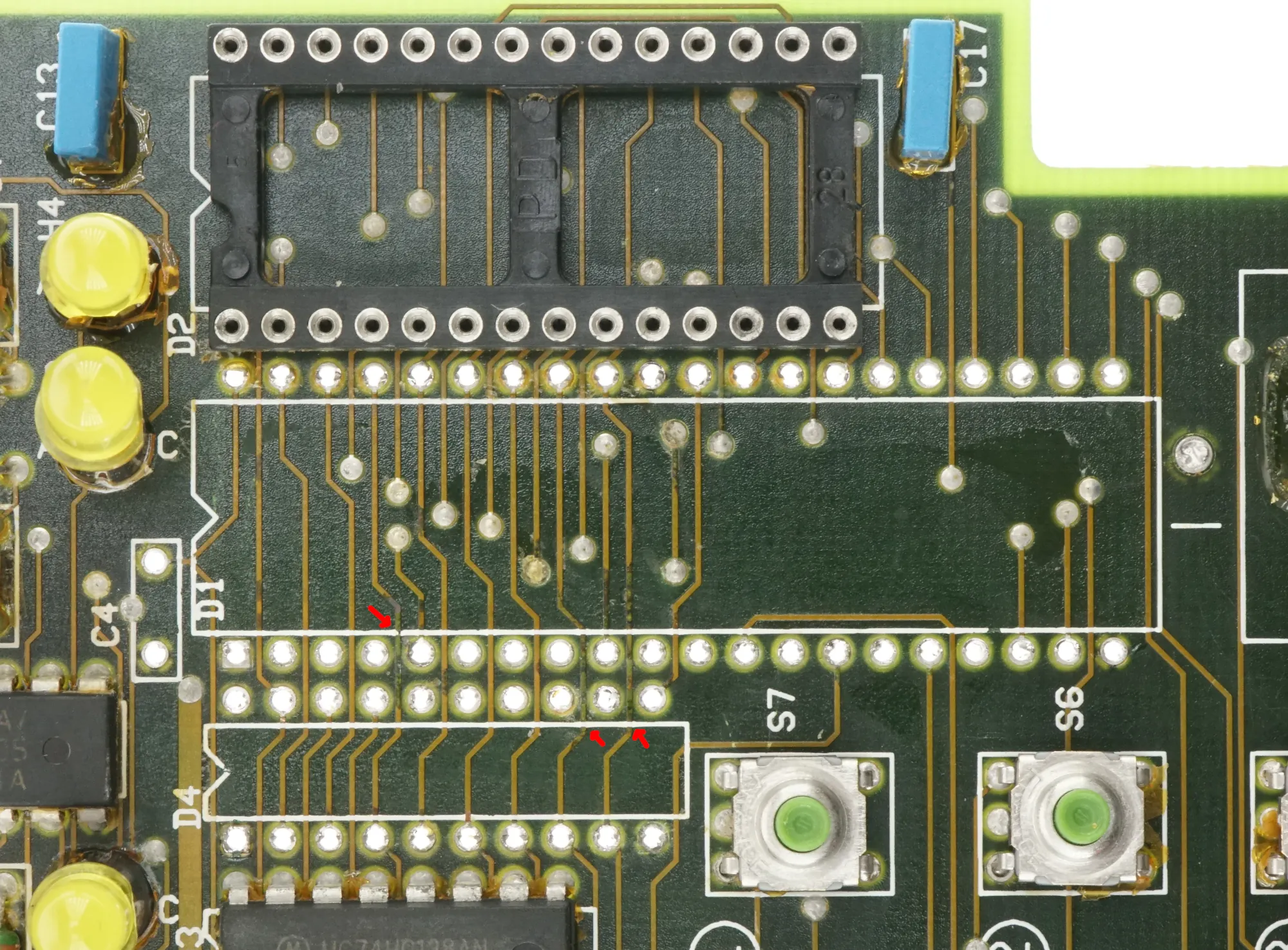
While examining the board closely, I noticed a couple traces that were corroded around the CPU. I pulled the processor and D4 (74HC573) to check them. They seem to measure fine (0.1 ohm or less). Nothing broken, but they may be a little flaky... board is definitely a lot cleaner looking now that the coating has been removed decently. Its really hard to get out from under the ICs though...
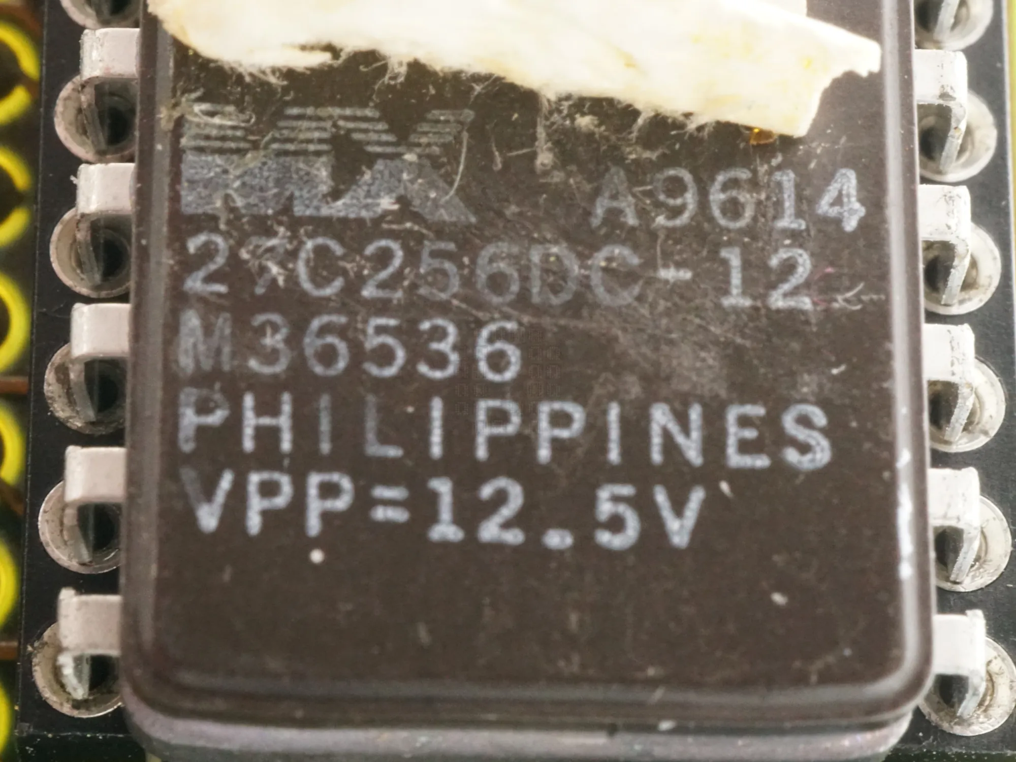
2023-02-24 ... a package finally arrives from china containing a brand new EGecu T56 Pro ROM reader/writer... hmm where is the nearest ROM to play with? why this circuit board has one... a MX 27C256DC-12. Well that's odd - Reader is giving me pin errors. Might just be the reader or the user. ...4 different ROMS later...nope. Reader is working nicely (it read an AWARD BIOS, two Macintosh LCIII ROMS and a couple ATTINY85 microcontrollers). Lets actually attempt to read the ROM and look at the data. Uhh...that ROM (ZIP-BIN, 32KB) doesn't look right. There are way too many FF bytes in there for my comfort. Sticker was still on the window though and board is normally housed in a black plastic enclosure. Perhaps it is a bad ROM chip or its been partially erased by UV? That's definitely problem number 3. Time to see if I can get a new ROM...
Old ROM above.
DeLaval Milking unit MU350 Instruction Sheet
2023-02-27: Now have new v2.41 ROM (ZIP-BIN, 32KB) burned on a ST M27C256B-15F1
2023-06-25 Update: Older ROM available v2.29 ROM (ZIP-BIN/HEX, 32KB)
2023-12-11 Update: Older ROM available v2.28A ROM (ZIP-BIN/HEX, 32KB) and here v2.31b ROM (ZIP-BIN/HEX, 32KB)
I think we have a working board again! No idea if the outputs and inputs work properly though... I need a full milking setup to check that. I also need to fix that diode yet...and verify that the battery retains settings.
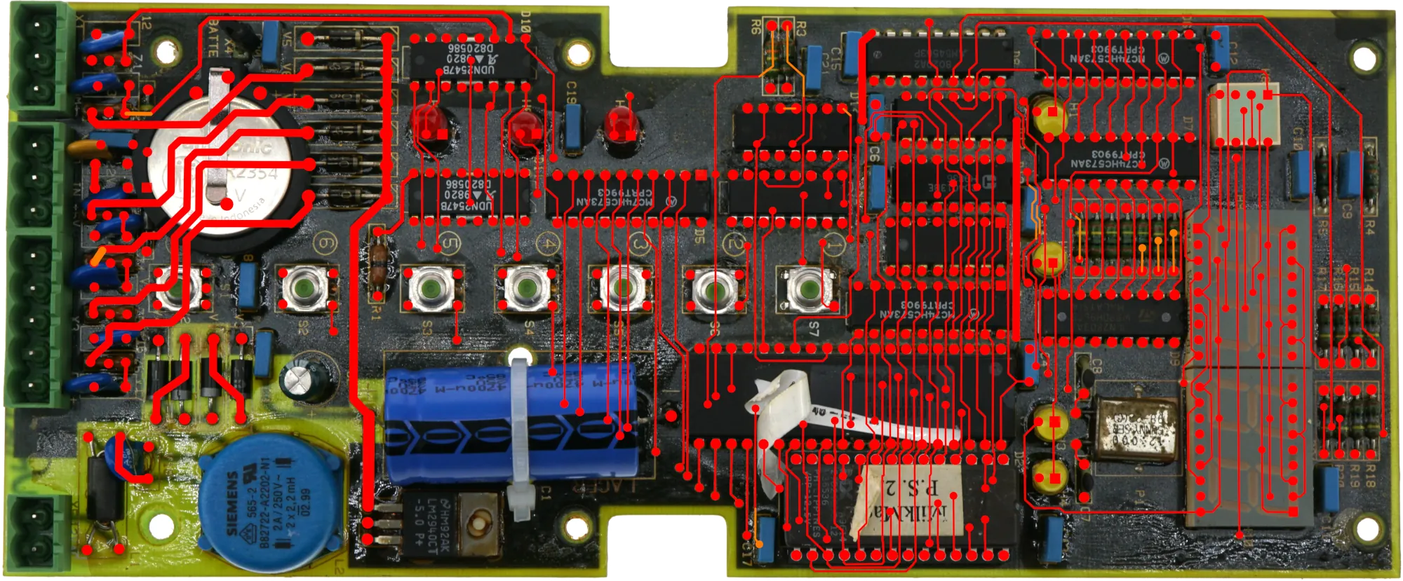
(Orange lines are continuity tested and not visually confirmed.)
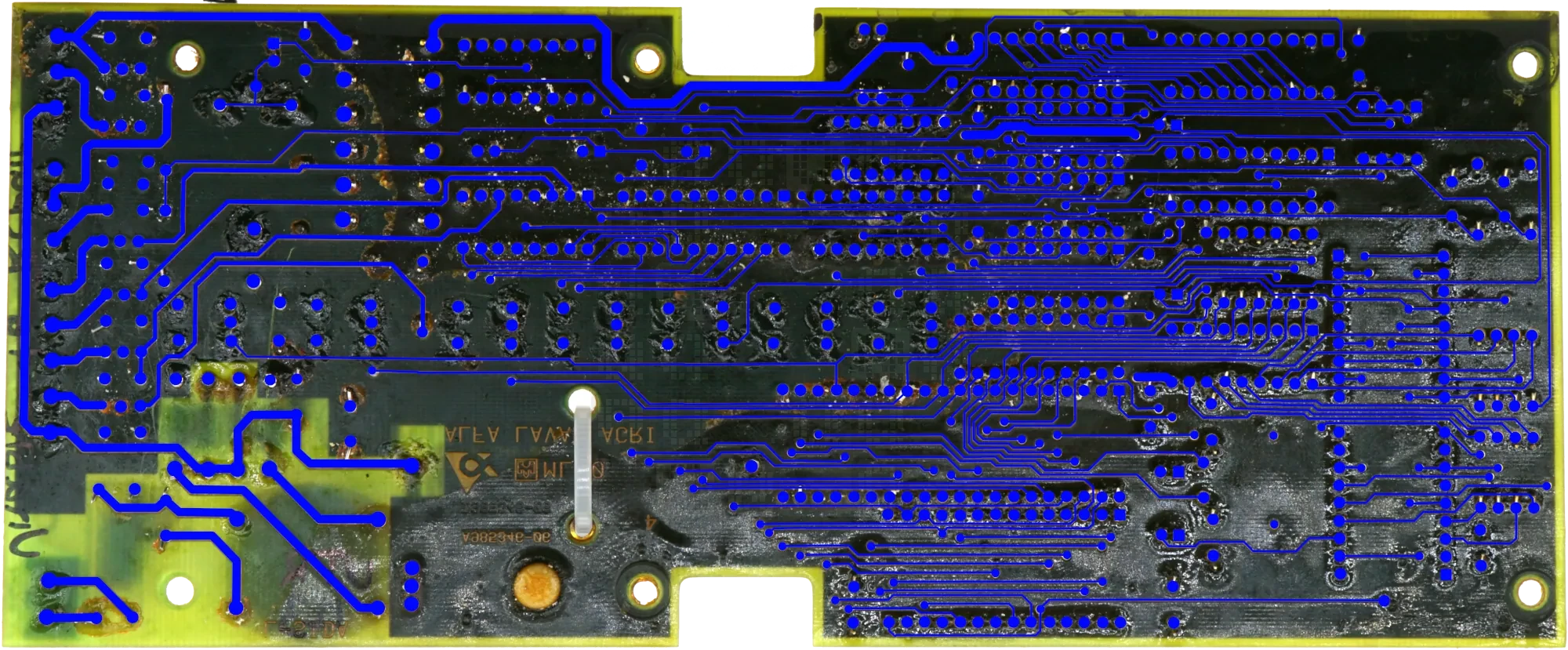
And since we're finishing up this project, I'll dump the rest of the info I've created/collected here as well. I posted the above to images before posting a link to this file (ZIP-.XCF-GIMP File, 115MB. Its rather large even scaled down. This file shows some of the circuit board traces. This is a four layer board, and the internal two layers are pretty much unknown. Not all the chips were removed from the board, so a lot of the Red (layer 1) copper is unknown. I did also create a couple electrical diagrams, which are pretty much worthless at this point, and are not included here for that reason.
As always, clicking on an image will bring up a larger version. Feel free to use the information above to repair your own boards; If reposting or using the information for any other purposes, please credit and link back to the original work (this page) and let us know about it. We also appreciate comments and corrections.
2023-05-05 Update: We got another stack of circuit boards to repair and as a consequence we now have some [mostly] completed electrical diagrams to share.
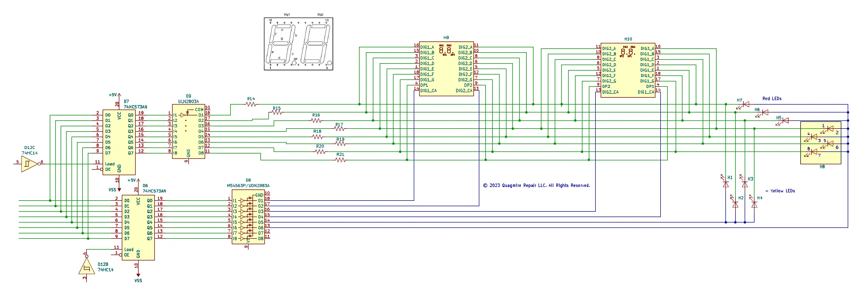
This diagram shows how the 7-segment displays are driven as well as the Red and Yellow LEDs. Clicking on this image will download a PDF.
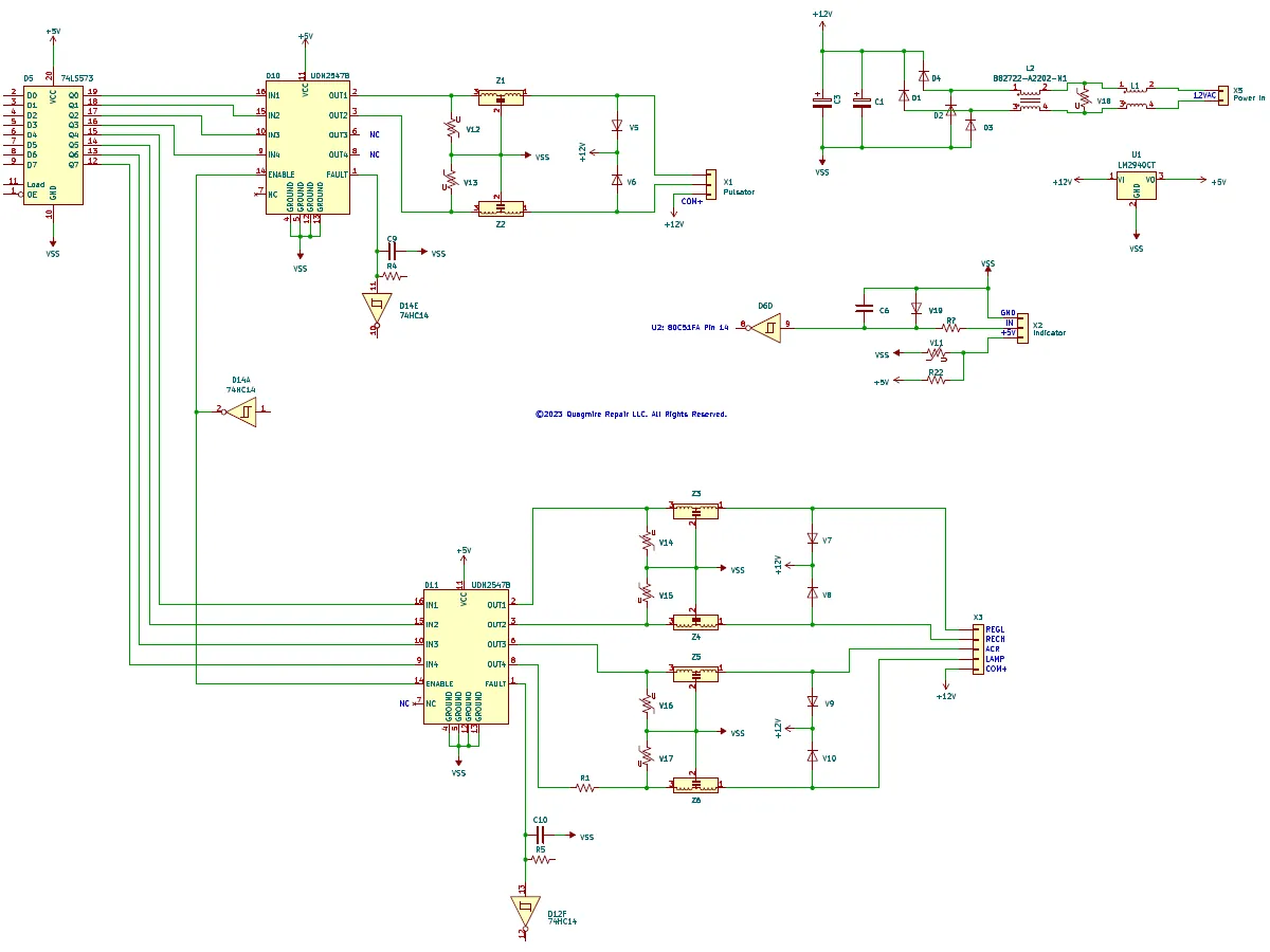
This diagram shows the Input and Outputs on this board, as well as the main power input circuit. Clicking on this image will download a PDF.
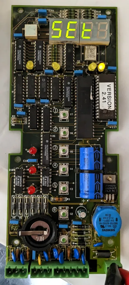
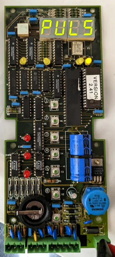
I also need to note here that there is a nice little test feature on the 2.41 ROM which shows ROM version and then cycles through each one of the display LEDs individually starting with the 4-segment bar-graph, 7-Segment Displays, Yellow LEDs, Red LEDS and then the board outputs. The test cycle ends with a button test, which also switches on and off the output terminals. S7 ends the test. To get to this test mode, Apply power to the board, push S7 until 'SEt' is shown. Push S6 until 'tESt' is shown. Press S5. 'yES' is then shown. Pushing S4 starts the test cycle.
Also updated red Copper picture above... As far as I'm aware, that copper layer is now complete.
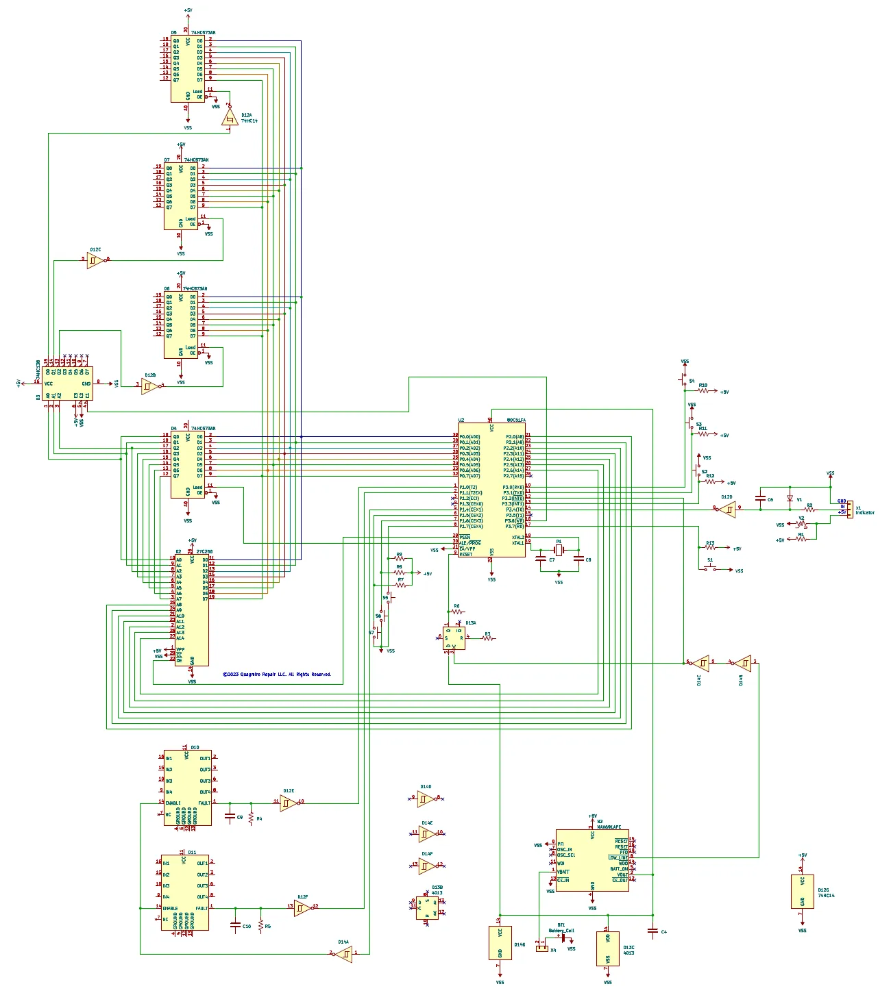
This diagram shows all the connections from the CPU. Clicking on this image will download a PDF.

