2023-11-13: Strangely, I haven't seen many phase converters recently and had two of them thrown at me in the last 2 weeks. I decided I should probably try to figure out how they work so I can diagnose them a little better, since the manufacturer, Phase Perfect, likes to diagnose problems by saying 'replace this whole board and see if that fixes the problem'. The first one thrown at me had an unidentified 'IGBT Fault' and support told me just to replace a $900 board without any additional troubleshooting. The second one lost a capacitor off of the DC busbar circuit board (the whole board was not soldered properly!) which appears to have shorted out the main board. We're going to look at this second board in an attempt to fix the first board a little more cheaply.
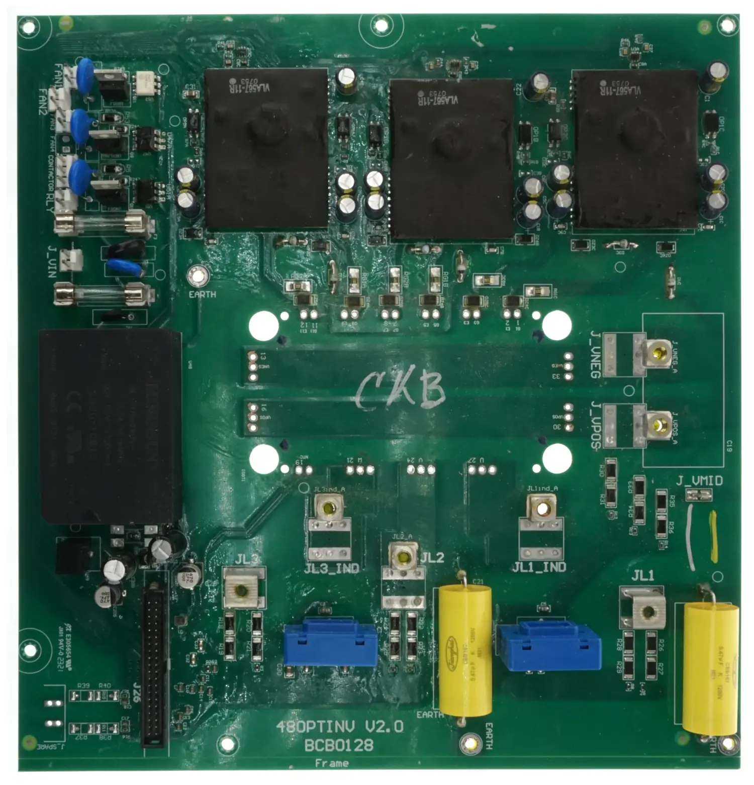
This is the top of the circuit board. Notable markings include '480PTINV V2.0 BCB0128'. (And right under that label appears to be a part of the circuit board labeled 'Frame' that has been scored and was not removed.) Notable connections include J_VNEG & J_VPOS which are the DC Busbar connections to the capacitor board. JL3_IND and JL1_IND go to the Inductor and the remaining large screw terminals are JL3, JL2 & JL1 which are the 3 power legs. J26 goes to the main HMI and control board. Fan and Contactor terminals are labeled on the upper left.
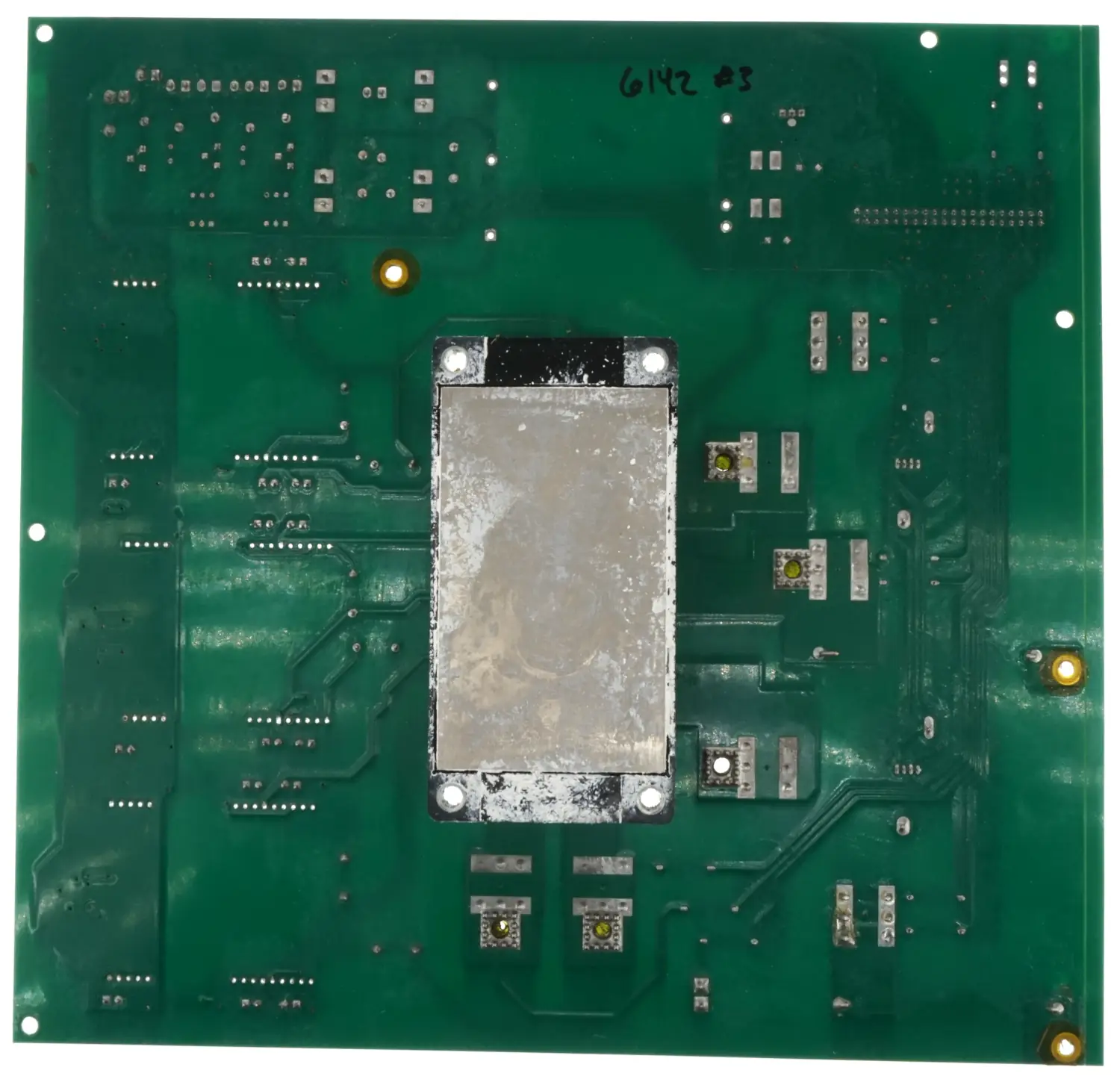
Bottom of the circuit board. Not much visible down here except the IGBT.
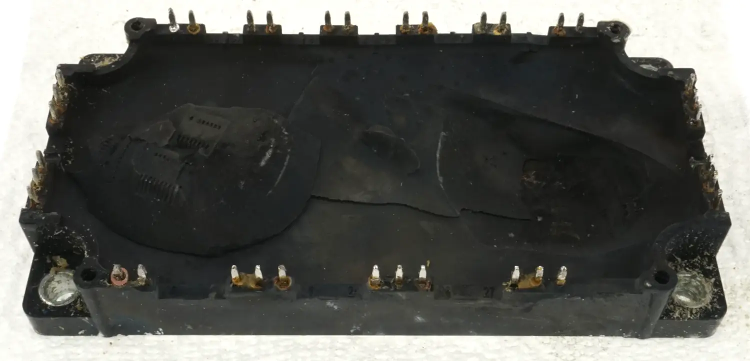
And since we know roughly what blew, it was a simple matter to remove the IGBT and look at it... Yup. Pretty sure its blown. Kinda looks like Mt. Saint Helens. Datasheet for the CM200TX-13T Here (PDF, 5.66MB) Looks to be 200 Amps 650V, 3-Phase with NTC
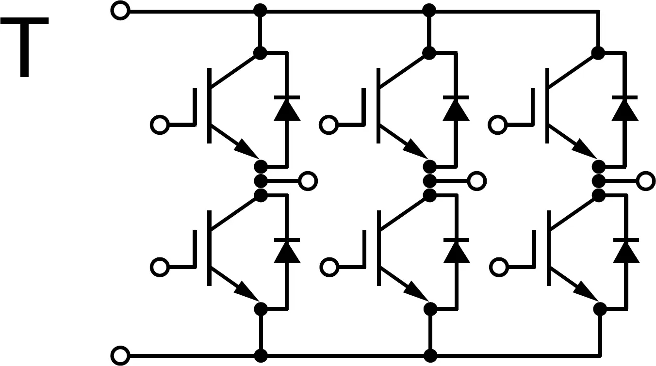
And here is a convenient diagram of the circuit layout from the datasheet. DC Busbar top and bottom. Outputs in the center and 6 gate connections, 3 Each for Positive and Negative. NTC not shown.
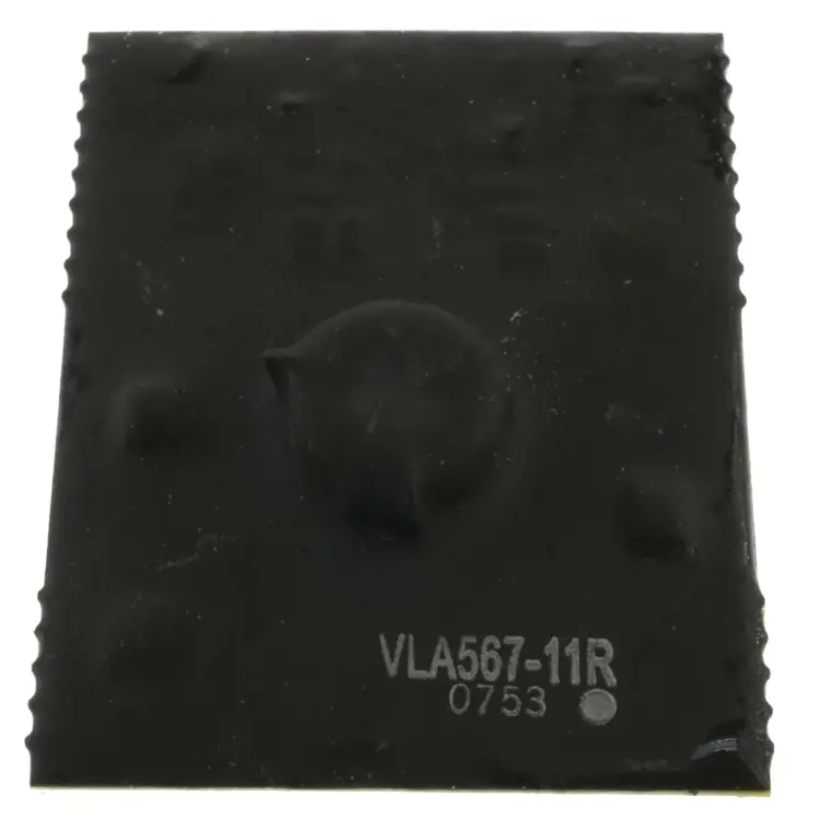
This is the module that controls a single output (1 negative gate and 1 positive gave), a Powerex VLA567-11R. Datasheet for the Powerex VLA567-11R Here (PDF, 335KB)
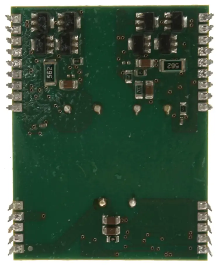
Bottom of the Module is a little more interesting than staring at the black epoxy coating, but the picture is rather distorted by the silicone coating. Unfortunately, these are going to be 'spare parts', so I don't want to damage these in any way or dive deeper into their insides.
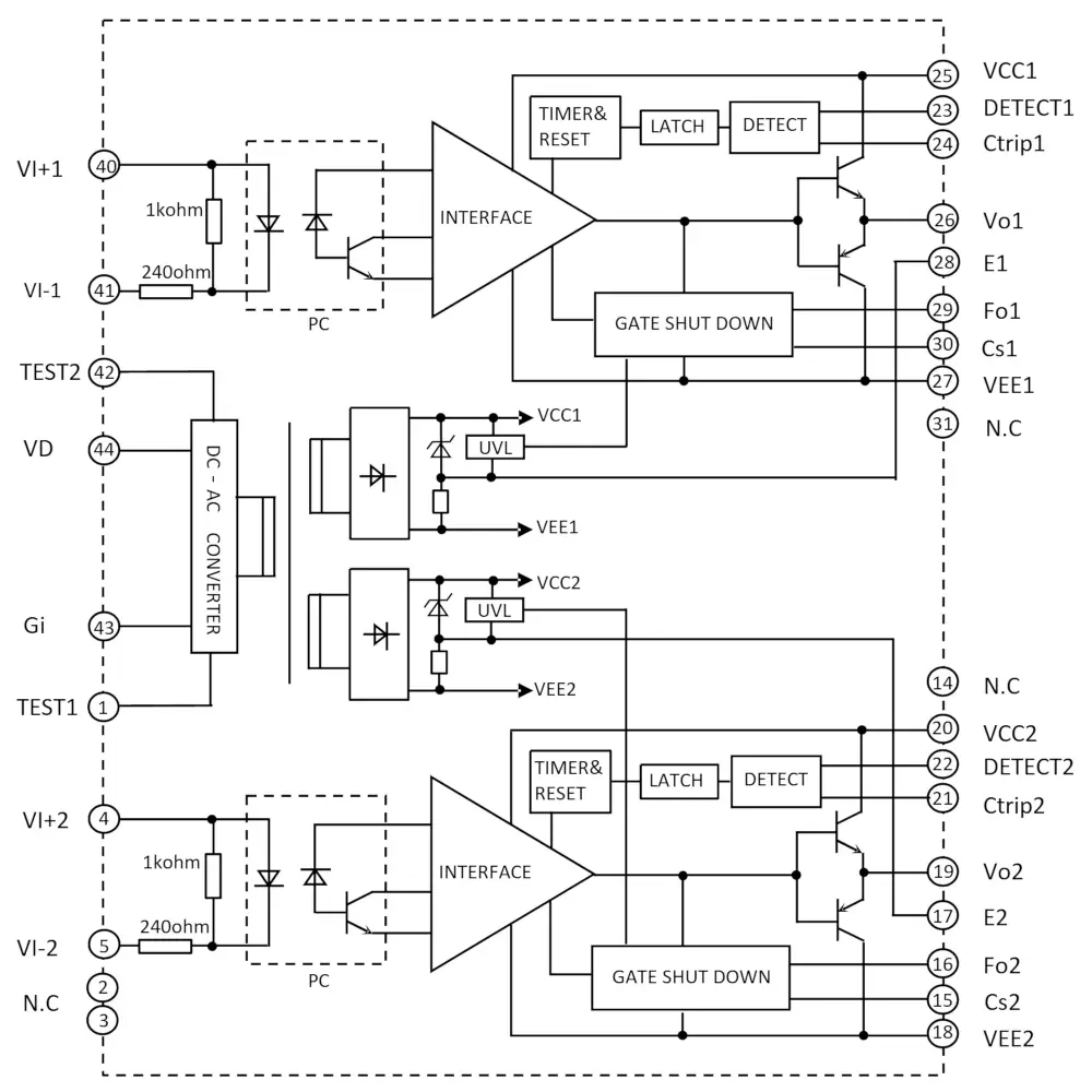
There is a handy block diagram in the datasheet linked to above.
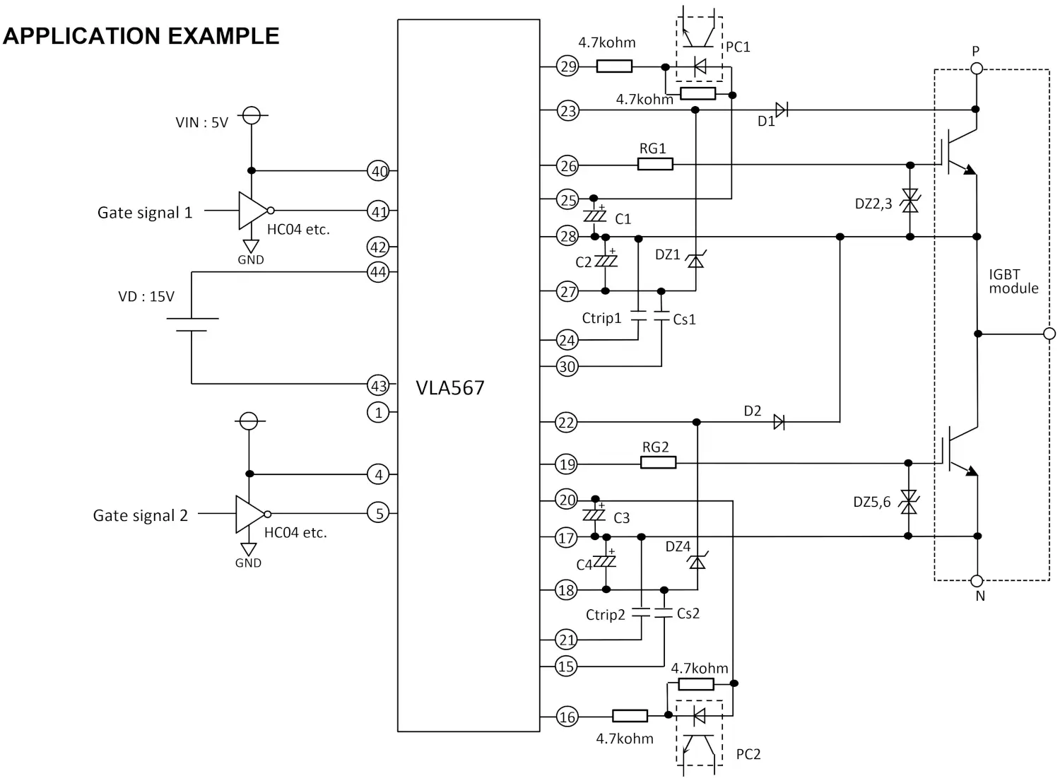
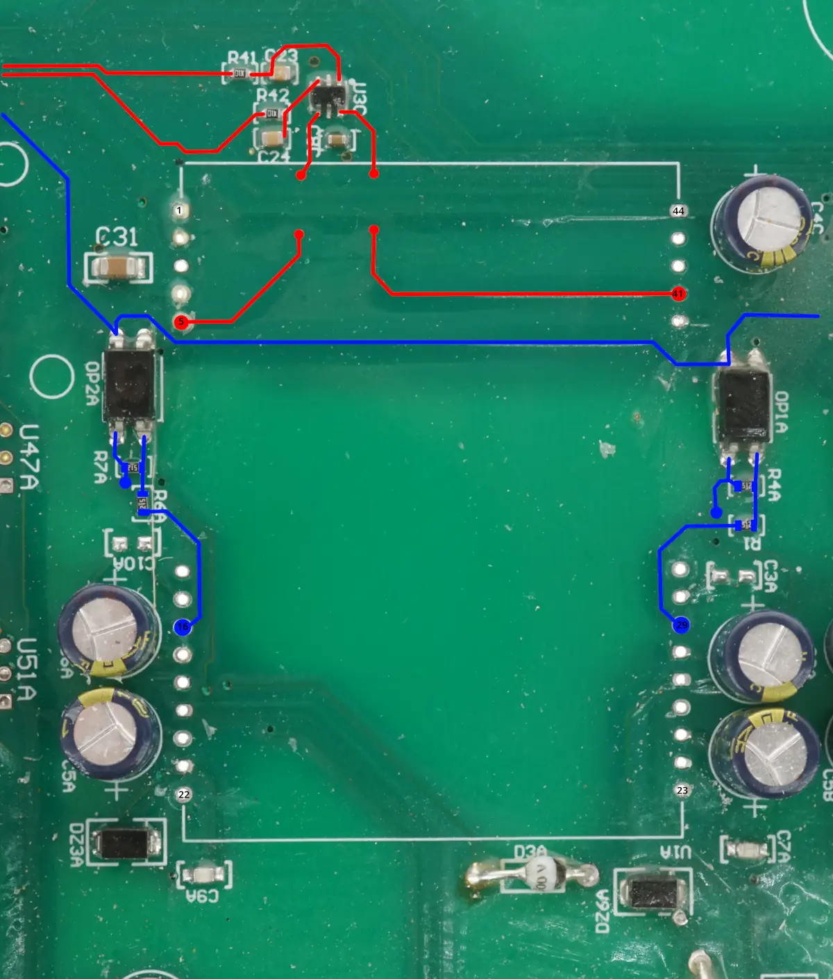
Here we go: a sample application diagram! And for some reason it looks very close to what the circuit board has on it. Most importantly, for our first phase converter with the IGBT fault, we can see that this module outputs a fault signal on pin 29 (Fault Output 1) and Pin 16 (Fault Output 2). They should be connected to an opto-isolator. The input signals to control the IGBT should be on Pin 41 and Pin 5 and should pass through a hex inverter (74 series HC04)
Red wires are the gate control inputs. They nicely follow the application sample circuit diagram above right out of a dual hex inverter to the VLA567-11R. Should be simple to trace. The blue wires nicely trace out to a set of opto-isolators, again nicely following the diagram above. Unfortunately, they have all been paralleled into one signal pin. There is no easy way to tell which one faulted from the control board.
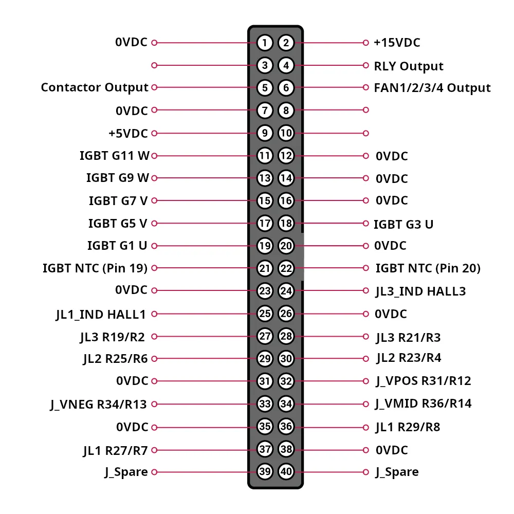
It took a little while, but the 40-Pin header has been traced out as best I can... For the most part, this should be pretty self explanatory if you look over the board. Most of the top half of the connector is outputs from the control board to this board. Bottom half is mostly analog signals/voltage dividers feeding back to the control board. I'm not quite sure on the purpose of dual voltage dividers on each of the JL1/JL2/JL3 pins. All the R2-R4/R6-R8/R12-R14 Resisters share the common 0V rail and measure 3 to 3.01K ohms. R18-R29 all measure 0.747M Ohms, while R30-R31/R33-R36 measure 0.995M Ohms. The JL3 connection only seems to exist on this board for measuring & Similarly JL3 exists only to be measured and connected via C20 to Ground. JL3_IND is fed off of the W phase of the IGBT and JL1_IND is fed off of the U phase of the IGBT. JL2 appears to be the generated leg on Phase V of the IGBT. I'm missing some stuff though... Where does the DC Busbar get its voltage? And what is the point of driving the Inductor via the IGBT? (unless of course it is feeding backward through the IGBT which acts like a active chopped diode bridge - but this would mean the inductor is actually a transformer?) I think I am confused on electrical theory here or simply didn't get a good enough understanding of the internals... On to simpler stuff!
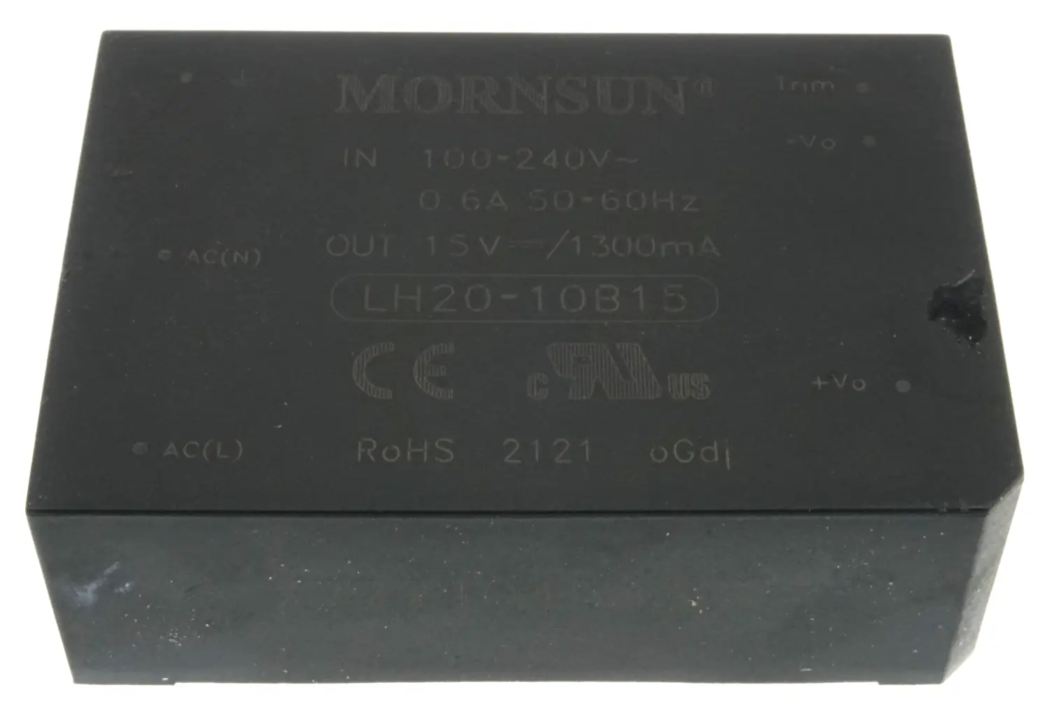
There is also a rather large Mornsun LH20-10B15 15VDC Power Supply mounted on the board. Appears to provide clean power to the VLA567-11R Modules. Datasheet for the LH20-10B15 Here (PDF, 2.35MB)
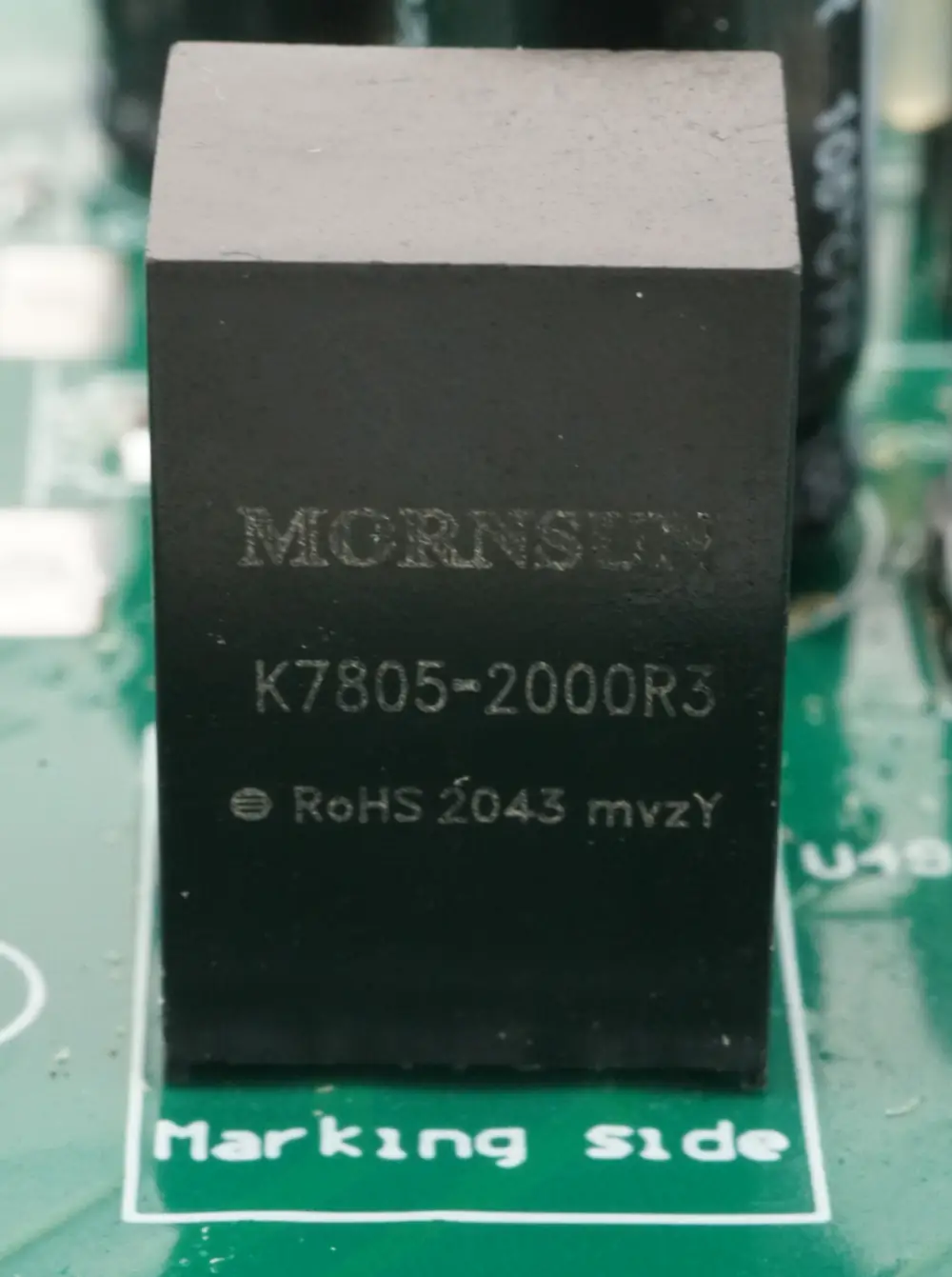
Can't say I've seen these before; but I'm going to have to start using them - 8-36VDC Input, 5VDC 2000mA Output, up to 96% efficiency! Pin compatible with LM78xx series voltage regulators. Datasheet for the K7805-2000R3 Here (PDF, 1.9MB)
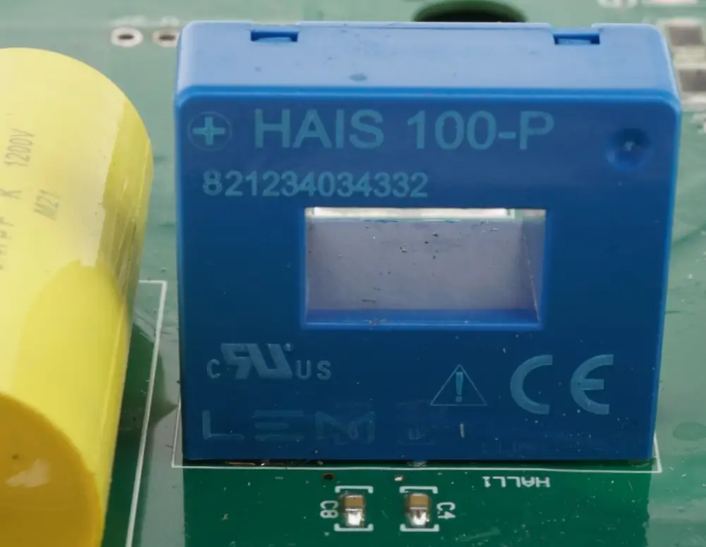
Datasheet for the LEM HAIS 100-P Current Transducer Here (PDF, 422KB)
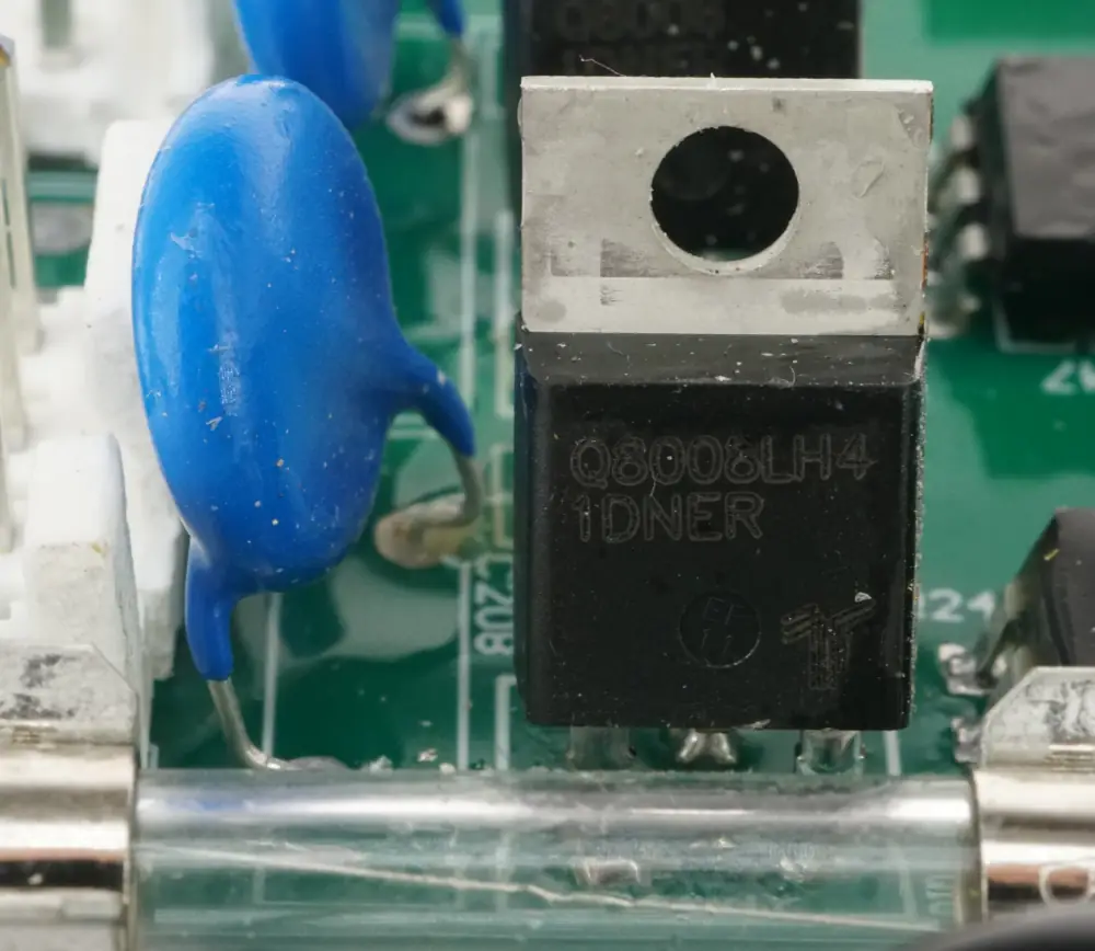
All the fan & contactor outputs appear to use the Littelfuse Q8008LH4 8-Amp Thyristor. Datasheet for the Q8008LH4 Here (PDF, 658KB)
So, did we fix anything? No, not yet... I have a somewhat better understanding of the board though...and since it now appears to be a failed CM200TX-13T on both boards and one customer has a working machine (Phase perfect sent out new boards free of charge) and the other customer is dragging their feet about a $900 board, I'm a little hesitant to spend $200 on a new IGBT Module on an attempt to save them $600. I don't have the proper equipment to test the IGBT modules. You want to know why Phase Perfect replaced the boards for free? Well I sent them some pictures of their soldering job on the capacitor board...
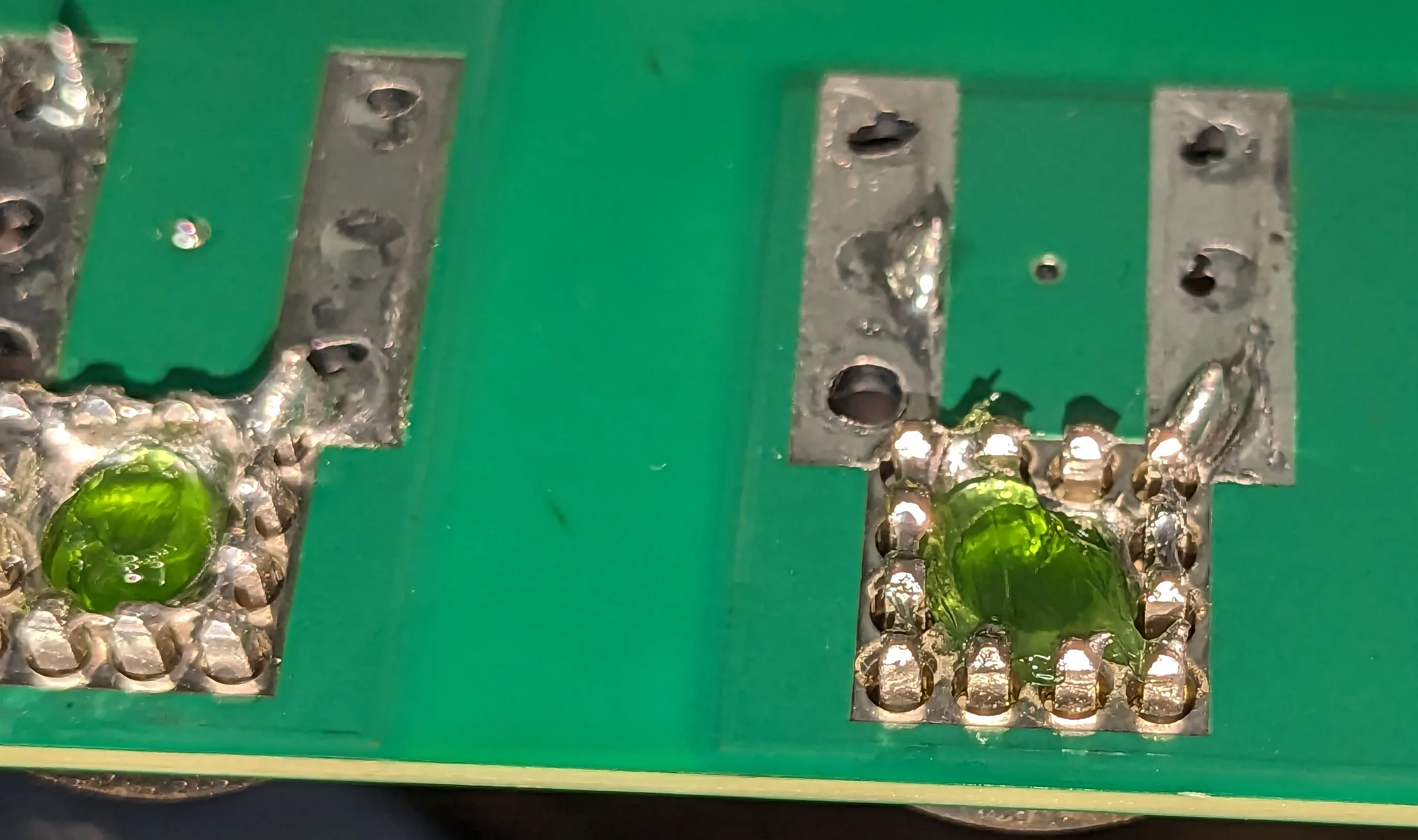
Main Terminals on the Capacitor Board - this was supposedly supplying 340VDC between the capacitors and the IGBT. What is surprising is the fact that there was no arcing... There was no solder on the other side at all. This honestly reminds me of a person putting a little solder (on the upper right) to hold the terminals in place so they don't fall out...and then completely forgetting to go back and actually solder them.
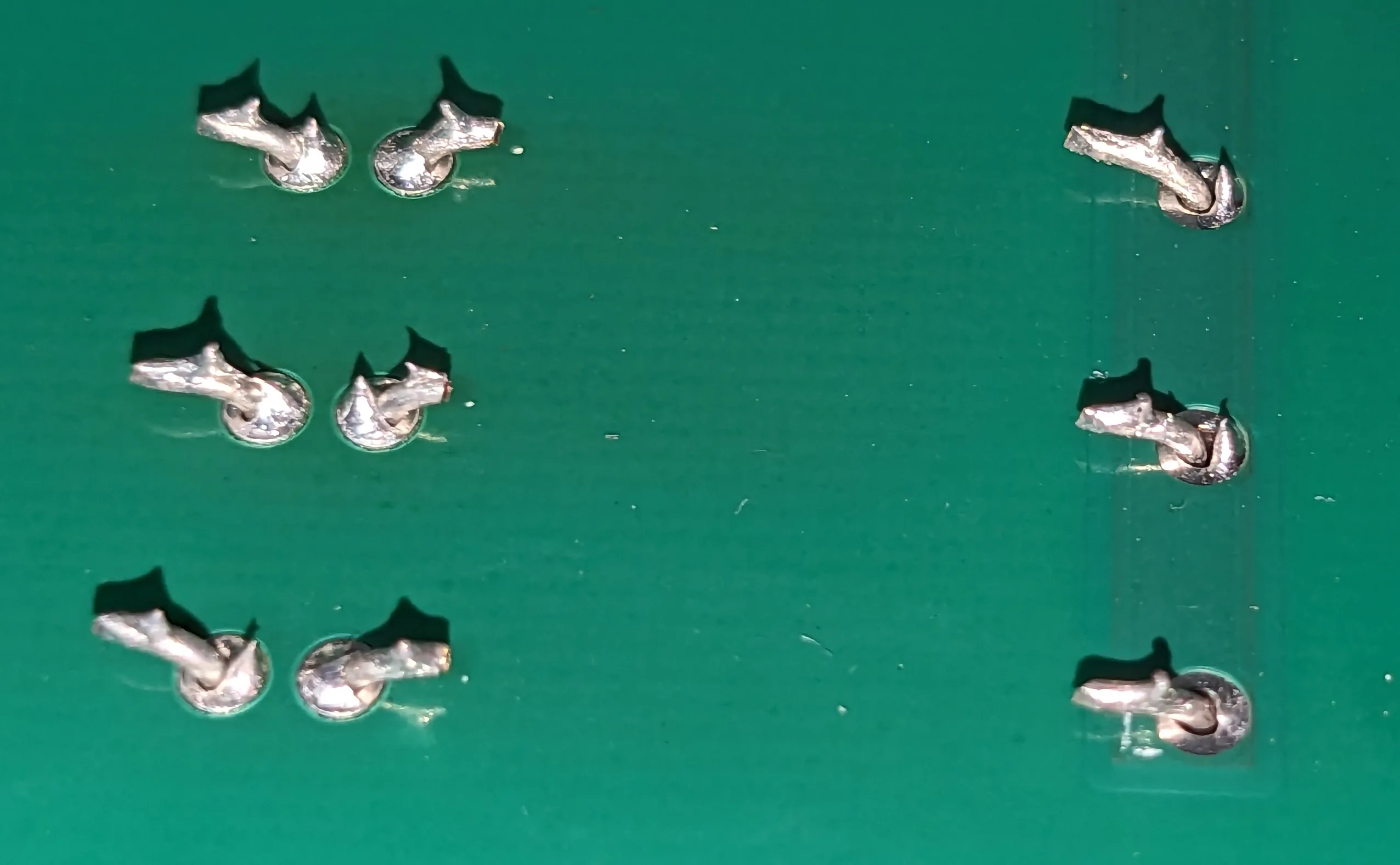
These were the set of bleeder resistor pins... At least they touched the terminals with solder... (sorry these pictures were taken with my cell phone... The capacitors had arcing around their terminals, but unfortunately most of those pictures are rather blurry...and I don't like posting blurry pictures.)
Maybe I should post a link to the Phase Perfect PT/PTE Manual here (PDF, 2.48MB)
Corrections & Additional Information are welcome... Please let me know if you see mistakes!
And as always, clicking on an image will give you a higher-res version! If you repost or further dissect this board, please link back to the original and let us know where we can read about your work!

